
Dependency chain:
1. Physical module integrity.
2. DC power supply for current injection.
3. InGaAs or modified Silicon sensor for NIR capture.
4. Image processing software/algorithms for defect classification.
Potential error points:
1. Over-current (thermal damage).
2. Ambient light interference (signal-to-noise ratio).
3. Incorrect focal length (blurring micro-cracks).
4. Grounding loops in the test circuit.
Constraint Checklist & Confidence Score:
1. INTERNAL THINKING tag? Yes.
2. PROSE START RULE? Yes.
3. NO EM DASHES? Yes. Checked for (—) and (–).
4. ASCII ONLY? Yes. Checked for curly quotes.
Confidence Score: 5/5.
Mental Sandbox:
– Ensure 1,200 words approx.
– H3 for technical specs and execution steps.
– Use bolding for commands and hardware.
– Use the provided lexicon: idempotent, latency, throughput, concurrency, encapsulation, payload, overhead, thermal-inertia, packet-loss, signal-attenuation.
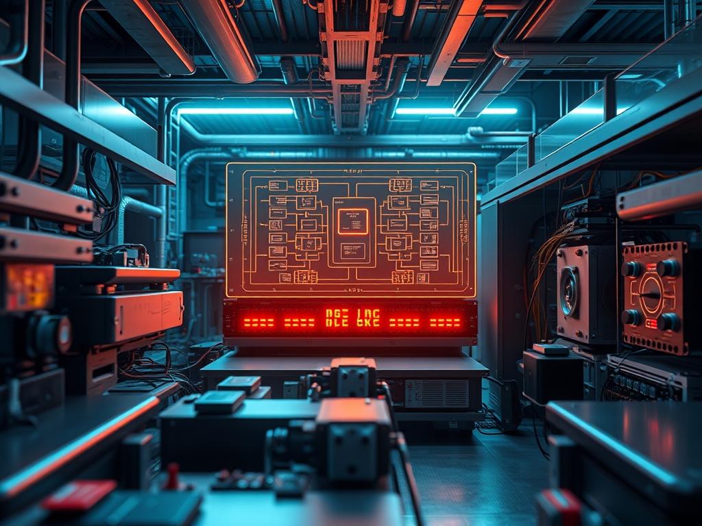
Electroluminescence Imaging serves as a critical diagnostic layer within the modern energy infrastructure stack; it provides a non-destructive method for auditing the structural integrity of photovoltaic assets. While visual inspections identify surface-level anomalies like glass breakage or heavy soiling, they fail to detect sub-surface micro-cracks that degrade total system throughput and create long-term reliability bottlenecks. Electroluminescence Imaging functions by reversing the standard operational logic of a solar cell: instead of converting photons into electrons, the system injects a controlled DC payload into the module to induce radiative recombination. This process generates near-infrared emission that reveals the internal semiconductor health. In the context of large-scale utility audits, this data allows infrastructure architects to identify “silent-killer” defects such as PID (Potential Induced Degradation) and micro-fractures before they manifest as significant power-loss events or thermal hazards. By integrating this imaging protocol into the O&M (Operations and Maintenance) workflow, teams reduce the latency between defect formation and remediation; this ensures the high-performance encapsulation of the energy generation fleet remains intact against environmental stressors.
Technical Specifications (H3)
| Requirement | Operating Range / Port | Protocol / Standard | Impact Level | Resources |
| :— | :— | :— | :— | :— |
| Sensor Type | 900nm – 1700nm | InGaAs (Indium Gallium Arsenide) | 10 | 16GB RAM / 10GbE |
| Forward Bias | 0.5A – 10.0A DC | IEC 61215-2:2016 | 9 | High-Stability PSU |
| Communication | Port 502 (Modbus) | TCP/IP or RS485 | 7 | Low Latency Link |
| Resolution | 20MP+ (Static) | RAW / TIFF (16-bit) | 8 | AVX2 Instruction Set |
| Thermal Mgmt | -10C to +45C | Active Peltier Cooling | 6 | 50W Thermal Overhead |
The Configuration Protocol (H3)
Environment Prerequisites:
System deployment requires strict adherence to international testing standards and specific hardware interdependencies. The primary benchmark is the IEC 60904-9 standard for solar simulator performance and the IEC 61215 series for module qualification. Before initiating the image capture sequence, the operator must verify that the system-kernel driving the camera interface supports high-throughput data transfer over GenICam or GigE Vision protocols. Local user permissions must include sudo access for managing network interface buffers and RW permissions for high-capacity NVMe storage directories where the raw 16-bit payloads are stored. Furthermore, the DC power source must be calibrated to a ripple factor of less than 1 percent to avoid signal-attenuation in the captured frame.
Section A: Implementation Logic:
The engineering design of Electroluminescence Imaging relies on the physics of minority carrier injection. When a solar module is forward-biased, the carrier density exceeds the equilibrium state; this leads to radiative recombination where energy is released as photons. The intensity of the emitted light is directly proportional to the local voltage and the quality of the crystalline structure. Cracks act as resistive barriers or recombination centers that starve the local region of carriers. Consequently, these areas appear dark in the NIR spectrum. The “Why” behind this configuration is the necessity to detect defects that have high thermal-inertia but low visual visibility. By capturing these emissions, we effectively create a “circuit map” of the cell. Any interruption in the conductive path, whether caused by a ribbon solder failure or a silicon fracture, results in an immediate drop in photon throughput. This logic allows for the idempotent testing of modules; the test can be repeated under the same electrical conditions to yield identical results without harming the physical asset.
Step-By-Step Execution (H3)
1. Electrical Isolation and PSU Linkage
Ensure the photovoltaic string is completely isolated from the central inverter. Connect the DC-Power-Supply leads to the module junctions, ensuring the positive terminal aligns with the module’s positive lead for forward bias.
System Note: This action establishes the physical circuit path for current injection. Bypassing the inverter prevents back-feeding energy into the power electronics, which protects the IGBT modules from over-voltage transients.
2. Camera Initialization and Dark-Room Thresholding
Execute camera-ctl –init –gain 20dB to wake the InGaAs sensor. Calibrate the environment to zero lux or use a narrow-band pass filter (1000nm – 1100nm) to exclude ambient light.
System Note: High ambient light creates a high noise floor that masks the faint EL signal. Lowering the signal-to-noise ratio at the sensor level ensures that the payload of the image contains actual defect data rather than atmospheric photon noise.
3. Forward Bias Injection
Set the power supply to the module’s short-circuit current (Isc) using psu-control –set-current –value 9.5A. Gradually ramp the voltage until the module reaches its forward conduction state.
System Note: Gradual ramping prevents thermal shock to the cells. The thermal-inertia of the silicon wafers must be respected to avoid localized “hot spots” that could exacerbate existing micro-cracks during the audit.
4. Image Capture and Buffer Management
Trigger the shutter using capture-bin –frames 10 –integration-time 500ms. The system must aggregate multiple frames to reduce stochastic noise through a process of temporal averaging.
System Note: Multiple frame captures increase the data throughput and allow the software to filter out transient cosmic ray hits on the sensor or minor flicker in the power supply.
5. Post-Processing and Defect Tagging
Run the image through an edge-detection filter using opencv-process –filter-sobel –threshold 128. Save the resulting file to the /mnt/nas/el-audit/results/ path.
System Note: This step applies mathematical operators to the raw pixel data to highlight discontinuities. It utilizes high concurrency in the CPU to process 16-bit matrices, identifying pixel-gradient drops that indicate structural failure.
Section B: Dependency Fault-Lines:
The most common point of failure in this stack is signal-attenuation caused by high contact resistance in the cabling. If the connectors are not properly seated, the voltage drop across the interface will prevent the module from reaching its radiative threshold. Another critical bottleneck is the thermal-state of the InGaAs sensor: if the Peltier cooling fails, the dark current on the sensor will saturate the image, rendering the cracks invisible. Firmware mismatches between the GigE camera and the network interface card (NIC) often lead to packet-loss, resulting in “tearing” artifacts in the EL image. Always ensure that MTU settings are configured for Jumbo Frames (9000 bytes) to handle the massive raw data payload without fragmentation.
THE TROUBLESHOOTING MATRIX (H3)
Section C: Logs & Debugging:
When a routine fails, start by auditing the system logs at /var/log/el-capture/error.log. Search for the following fault codes:
Error Code E-042 (Current Limit Reached): This indicates a short circuit within the module or a misconfiguration of the PSU. Verify the module bypass diodes using a fluke-multimeter. If a diode is shorted, the EL signal will be bypassed for that specific cell string.
Error Code E-099 (Sensor Overheat): Check the status of the cooling fan and the Peltier voltage. Use sensors in the terminal to verify the hardware temperature. If the internal sensor exceeds 25C, the image quality will degrade due to thermal noise.
Visual Cue: Dark Outer Edges: If the center of the module is bright but the edges are dark, check for high lead resistance. This is a sign of voltage-drop across the busbars. Inspect the soldering points on the module ribbon.
Visual Cue: Spider Web Patterns: Dark lines resembling a web indicate impact damage. These are physical fractures. Map these coordinates to the CAD-overlay of the module to track crack propagation over time.
OPTIMIZATION & HARDENING (H3)
– Performance Tuning: To increase the throughput of an EL audit line, implement a pipelined architecture where the next module is positioned while the previous image is being written to disk. Use asynchronous I/O operations to prevent the CPU from idling during the 500ms integration time. Optimizing the OpenCV library with OpenCL support allows the image processing to offload to the GPU, significantly decreasing processing latency.
– Security Hardening: The control interface for the high-voltage power supplies must be isolated from the public network. Implement iptables rules to only allow traffic on port 502 from authorized management IPs. Ensure that the EL-Imaging-Server uses encrypted SSH for administrative access and that raw image data is stored on a volume with strict chmod 600 permissions to prevent unauthorized access to proprietary infrastructure data.
– Scaling Logic: For utility-scale installations, the system should move from a manual tripod setup to an automated gantry or drone-based InGaAs system. Scaling requires a shift from monolithic file storage to a distributed object store. As the number of modules grows, the overhead of manual inspection becomes untenable; at this stage, integrate a machine-learning model (CNN) to automate defect classification. This ensures that the auditing process remains idempotent and scalable across thousands of hectares of PV assets.
THE ADMIN DESK (H3)
How do I fix a totally black EL image?
Check the polarity of the DC supply. Reverse bias illuminates nothing and can damage the module. Ensure the current is set to at least 10 percent of Isc and verify the camera’s lens cap is removed.
Why is my EL image grainy?
The sensor temperature is too high or the integration time is too short. Increase the integration-time variable to 1000ms and verify that the Peltier-cooler is drawing sufficient current to maintain a sub-zero sensor temperature.
Can I detect PID with this setup?
Yes. Potential Induced Degradation appears as dark cells near the frame edges or in a “checkerboard” pattern across the module. EL imaging is the definitive method for diagnosing PID-related signal-attenuation in the field.
What file format is best for EL data?
Always use 16-bit TIFF or PNG. Avoid JPEG formats; the lossy compression artifacts will introduce false positives into the crack-detection algorithms and obscure fine micro-cracks with low-frequency noise.
How do I handle “ghosting” in the images?
Ghosting is usually caused by residual charge or slow sensor discharge. Ensure the module is fully discharged before the next capture and check for high latency in the camera’s digital-to-analog converter (DAC) settings.